
Why China TaC Coated Susceptor Is Gaining Traction in Advanced Semiconductor Manufacturing
2026-11-19
The push to improve yield in advanced semiconductor manufacturing is forcing a closer look at every component inside the process chamber. Tantalum carbide coated susceptors have become a focal point, especially as China-based suppliers demonstrate that high-performance TaC coatings can be delivered at scale without the long lead times that once held back adoption. Semicorex follows this shift closely, and the implications for thermal control, contamination risk, and fab economics are far from ordinary.
TaC Coatings Quietly Solve the Carbon Contamination Problem in High-Temperature Epitaxy
In high-temperature epitaxy, graphite fixtures are convenient and inexpensive, but they have a habit of leaking carbon into the growth environment. The problem rarely announces itself; it shows up later as background doping, uneven nucleation, or films that look acceptable but drift out of spec. TaC coatings take a different route by sealing the graphite surface instead of asking process engineers to compensate with longer bakes or adjusted gas flows.
Once applied, the coating converts the exposed graphite into a dense, stable carbide layer. That layer does not flake the way bare graphite does after repeated thermal cycling, and it suppresses the steady release of carbon-bearing species that would otherwise find their way into the wafer. For SiC and III-nitride growth, the difference is often invisible in a single run but obvious in accumulated defect maps and maintenance logs.
The quiet part is that TaC does not change the headline parameters of the recipe. It simply removes a source of variability that had been accepted as normal for years. Teams that switch over tend to notice fewer carbon-related particles, longer intervals between cleaning, and less drift in electrical properties from batch to batch.
China’s Domestic SiC Supply Chain Creates an Opening for Tantalum Carbide Alternatives
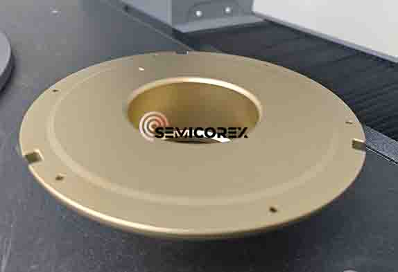
The rapid expansion of China's domestic silicon carbide wafer capacity has started to shift purchasing logic in the high-temperature consumables segment. Tantalum carbide coatings have long been the default choice for crystal growth fixtures, but their concentrated supply base and volatile pricing sit awkwardly with the cost targets now being pushed through Chinese production lines. As a result, materials teams are giving serious evaluation time to alternative carbides and multilayer coatings that were previously dismissed as second-tier options.
These alternatives are not being positioned as simple substitutions. Suppliers are adjusting carbon-to-metal ratios, modifying deposition parameters, and adding intermediate layers to address the weak points that once made tantalum carbide hard to replace, particularly edge peeling and particulate contamination during long growth runs. In some pilot campaigns, the improved coatings have shown acceptable stability across repeated heating cycles, which matters more to production engineers than nominal material properties.
The move toward larger-diameter SiC substrates adds another incentive. Eight-inch crystal growth requires bigger hot zones and consumes more protective coatings per batch, so even a modest per-part cost reduction becomes significant at scale. Domestic equipment makers, growers, and coating shops are now running joint validation programs, and that collaborative pressure is quietly eroding the assumption that tantalum carbide must remain the only viable material in the thermal field.
Thermal Stability Beyond 1,600°C Changes the Susceptor Replacement Calculus
The assumption that a susceptor needs replacement after a set number of heating cycles quietly falls apart when you push past 1,600°C. At lower temperatures, surface oxidation and gradual grain growth are the usual culprits, and they follow a predictable rhythm. Above 1,600°C, however, the failure mode shifts. Sublimation at the edges, localized recrystallization in high-flux zones, and the slow migration of impurities toward the hottest face begin to dominate. These are not linear processes, so a simple count of cycles stops being a useful proxy for remaining life. Operators who keep relying on old replacement schedules end up swapping parts that still have months of service left, or worse, running a susceptor past the point where its emissivity has drifted enough to throw off temperature uniformity.
What actually changes above 1,600°C is the cost-benefit of in-situ monitoring versus scheduled replacement. A susceptor that survives 2,000 cycles at 1,400°C might fail in 300 at 1,700°C, but not because it has become uniformly weaker. Instead, small zones near the gas inlet or the wafer edge develop different thermal expansion behavior, creating stress concentrations that are nearly invisible on a bulk resistance check. This is where the replacement calculus shifts from a calendar-driven decision to a condition-driven one. You are no longer asking "how many runs has this part seen?" but "where is the thermal gradient starting to bend the part's shape?" The answer often comes from a combination of pyrometry drift, weight loss per run, and a quick visual scan for the telltale dulling that signals surface stoichiometry change.
Suppliers are catching on, but the language is still catching up. Some now offer susceptors with a slightly higher porosity near the back face to slow impurity migration, while others tune the grain structure to resist creep at extreme soak times. The practical takeaway is less about finding a universal replacement interval and more about abandoning the idea that one exists. A susceptor that runs mostly at 1,650°C with short ramps may outlast one that cycles between 1,200°C and 1,700°C, even if both log the same total hours above 1,600°C. Thermal history, not just peak temperature, writes the real failure curve. Teams that treat the susceptor as a consumable with a fixed lifespan are leaving either performance or budget on the table.
Lower Metal Impurity Levels Are Reshaping Yield Targets for Power Devices
For power devices, the conversation around yield has shifted from gross defect density to the subtle electrical signatures left by trace metals. Iron, copper, and nickel contamination at levels that were once considered background noise now show up as elevated leakage currents, shifted threshold voltages, and premature breakdown in IGBTs and superjunction MOSFETs. As fabs push metal impurity levels below 1E10 atoms/cm², the yield targets themselves are being recalibrated: a wafer that passes parametric tests today may still carry enough latent contamination to fail after thermal cycling or high-temperature reverse bias.
The impact is especially visible in wide-bandgap devices. Silicon carbide and gallium nitride structures operate at higher electric fields, so a metal precipitate located near the channel or in the drift region creates a localized field crowding that silicon would tolerate more easily. Process teams now track contamination by device area and field strength rather than by blanket wafer maps, which means yield models have to account for the statistical probability of a killer particle landing in a high-field zone. This has made edge-die exclusion, backside treatments, and wet bench sequencing part of the yield equation, not just defect inspection.
What emerges is a tighter link between contamination control and economic wafer sort. Instead of setting yield targets from historical averages, fabs are starting from the electrical distribution of known-good die and working backward to acceptable metal budgets per layer. The result is that a two percent yield gain in a power device line can come from eliminating a single wet clean residue, and the targets keep moving as lower impurity baselines expose other failure modes that were previously masked.
Wafer Warpage and Slip Reduction Give TaC a Practical Edge in Thin-Film Uniformity
Wafer bow and slip are early signals that thermal control is drifting out of range. TaC-coated hardware suppresses both by reducing the thermal expansion mismatch at the wafer support interface. Instead of the wafer lifting slightly from the pocket, it remains seated while the reactor approaches process temperature, so stress gradients are less likely to concentrate at the wafer edge.
That extra flatness has a direct influence on thin-film uniformity. A wafer that stays in contact with the susceptor across the full diameter sees more predictable heat transfer and a smoother boundary layer over the surface. Localized temperature swings that normally produce thicker deposits near the edge or central thinning become less pronounced. The result is a tighter distribution of film thickness and dopant incorporation without constant recipe compensation.
TaC also keeps the surface from degrading after repeated exposure to hydrogen, ammonia, or silicon-containing precursors. A stable surface avoids the gradual roughening that can change emissivity and reintroduce thermal non-uniformity over time. For high-volume epi lines, that means fewer interrupts for reclaim or adjustment and better run-to-run consistency.
Why Process Engineers Are Revisiting Susceptor Materials for Next-Gen Logic and Memory
Process engineers are not swapping susceptor materials because the old ones stopped working. The shift is more subtle: defect budgets on advanced logic and memory lines have shrunk to the point where small changes in wafer temperature uniformity or particle shedding from a coated graphite carrier now show up directly in yield. Traditional SiC-coated graphite still dominates, but the repeated thermal cycling in high-temperature epitaxy and selective deposition steps has exposed microcracking, edge erosion, and shifts in surface emissivity that were acceptable a few nodes ago but are no longer invisible in inline metrology.
Part of the renewed interest comes down to device geometry. Gate-all-around architectures and high-aspect-ratio 3D NAND stacks are more sensitive to local temperature gradients during deposition because small variations in film thickness or stress can distort stacked features or alter channel mobility. Engineers are therefore testing alternatives such as solid sintered SiC, aluminum nitride, and tantalum-based coatings that promise better thermal stability and lower particle generation over longer campaign lengths. The evaluation is practical rather than theoretical: a material only moves forward if it survives repeated ramp-up and ramp-down cycles without flaking, warping, or changing how heat couples into the backside of the wafer.
There is also a contamination angle that gets less attention. As logic and memory processes introduce new metal precursors and halide-based etch or clean steps, trace metals from susceptor materials can interact with gas phase species in ways that leave subtle residues on wafer edges or backsides. This pushes teams toward fully dense CVD SiC layers or alternative ceramics that do not expose porous graphite after a few hundred wafers. In that environment, the selection criterion is rarely catalog purity alone; it is the stability of the surface after it has been aged in the actual process chemistry.
FAQ
Tantalum carbide resists attack from ammonia and hydrogen at high temperatures, which helps keep the susceptor surface stable during repeated GaN or SiC deposition cycles. It also limits particle generation and unwanted doping drift.
Domestic wafer fab expansion has pushed local equipment and consumable vendors to qualify alternative sources. Some Chinese manufacturers now offer denser coatings and faster re-coating services, which shortens lead times for fabs in the region.
The coating has high thermal conductivity and remains dimensionally stable under thermal cycling. More consistent heat transfer across the pocket area reduces wafer bow and improves thickness uniformity of the deposited epi layer.
The shift is most visible in gallium nitride power and RF device production, silicon carbide epitaxy, and to a lesser extent in some LED lines where high-temperature ammonia processes are common.
Better chemical vapor infiltration and spraying methods have reduced porosity and delamination. Suppliers also run more demanding thermal shock tests and provide data on particle counts and resistivity, which makes qualification easier for device makers.
Local sourcing cuts freight time, import duties, and inventory tied up in spare susceptors. When coating performance is comparable, fabs often prefer a nearby vendor that can inspect, recoat, and return parts within a shorter cycle.
Some overseas fabs still require longer lifetime data across multiple process regimes and want independent verification of purity and micro-cracking resistance. Documentation and process-matching support can also be less mature than established suppliers.
They should review coating thickness mapping, porosity, surface roughness after baking, resistance to ammonia etching, and particle performance after repeated thermal cycles. Requesting a pilot run on a production tool with standard process gas flows is usually more informative than relying only on coupon data.
Conclusion
The shift toward tantalum carbide coated susceptors in China isn't driven by a single breakthrough; it's a convergence of production headaches that conventional graphite and SiC-coated parts have not fully resolved. In high-temperature epitaxy, carbon outgassing from exposed graphite changes local doping and introduces particles that are hard to trace until yield drops. TaC coatings create a much more inert surface, cutting that contamination path early in the process. At the same time, China's expanding domestic SiC wafer and epi capacity has made suppliers less willing to accept the long lead times and variable quality of imported coated parts. A local TaC alternative fits that supply chain pressure because it allows fabs to qualify a stable, repeatable surface without being hostage to a single overseas source. The material also holds up above 1,600°C without the rapid degradation that forces frequent susceptor swaps, so maintenance windows stretch further and chamber conditions stay more consistent run to run.
Beyond cleanliness and uptime, the practical yield impact shows up in lower metal impurity levels and reduced wafer stress. Metallic contamination from a degrading susceptor can compromise gate oxide integrity and shift threshold voltages, which matters as power devices move to tighter performance bins. TaC's thermal and chemical stability keeps those impurity contributions low enough that process engineers can separate susceptor-related defects from other variability sources. On the wafer side, better resistance to thermal shock and more uniform heat distribution reduce slip lines and warpage during ramp-up and ramp-down. That leads to more uniform thin-film thickness across the wafer, an advantage that becomes harder to ignore when epi thickness budgets shrink for advanced logic and memory. Engineers are revisiting susceptor materials not because TaC is new, but because the cost of ignoring these interactions has risen.
Contact Us
Contact Person: Svenja Wei
Email: [email protected]
Tel/WhatsApp: +8613567891907
Website: https://www.semicorex.com